


- Industry: Communications / Electronics
- Time: 2026/12/15 - 12/17 (Tues To Thur Total 3 Days) Error Correction
- Address: Shanghai Shanghai New International Expo Center (SNIEC) ChinaShanghaiPudong New Area No. 2345 Longyang Road, Pudong New Area, Shanghai
- Sponsor:2026 Shanghai International Semiconductor Industry Chain Exhibition
- Organizer:2026 Shanghai International Semiconductor Industry Chain Exhibition


- Telephone:157 2131 7652
- Contact:Xu Yang
- Mobile:157 2131 7652
- Address:No. 2345 Longyang Road, Pudong New Area, Shanghai

INTRODUCTION


2026 Shanghai International Semiconductor Industry Chain Exhibition
Date: December 15-17, 2026
Location: Shanghai New International Expo Center
Development prospects:
Semiconductor technology is a core part of modern technology, with a wide range of applications involving many different fields. Semiconductor technology also plays a very important role in fields such as new energy, electric vehicles, and digital economy. During the 14th Five Year Plan period, China will focus on some key core technologies and cutting-edge basic research in the fields of integrated circuits, software, high-end chips, and new generation semiconductor technology. Support will be provided through national key research and development programs, fully leveraging the innovative status of enterprises and promoting deep integration of industry, academia, and research. In the future, China will take SiC and GaN materials, which have relatively mature technology and product development, as the entry point to rapidly expand the scale of the third-generation semiconductor industry. Focus on key links in the third-generation semiconductor industry chain, such as materials, epitaxy, chips, devices, packaging, equipment, and applications, and strengthen industry university research cooperation.
With the continuous research and technological breakthroughs in the domestic semiconductor industry, China has become one of the largest consumer countries in the global semiconductor manufacturing industry. In the next few years, China will become the world's largest semiconductor market. This also means that China will play an important role in promoting the development of the global semiconductor industry and become a key development trend in the global semiconductor industry in the coming years. The semiconductor industry will continue to maintain stable growth in the coming years and play an increasingly important role in the global economy. According to the "Opinions on Accelerating Industrial Transformation and Upgrading, and Building a World Class Integrated Circuit Design and Manufacturing Base" issued by the Ministry of Industry and Information Technology (referred to as the "Thirteen Articles"), more than 100 important enterprises in China will be approved for layout in the next five years. This will further promote the development of China's semiconductor industry and create more opportunities for domestic enterprises. Under this new development opportunity, China's semiconductor industry will usher in a broader market space and more opportunities for cooperation.
Industry Summit:
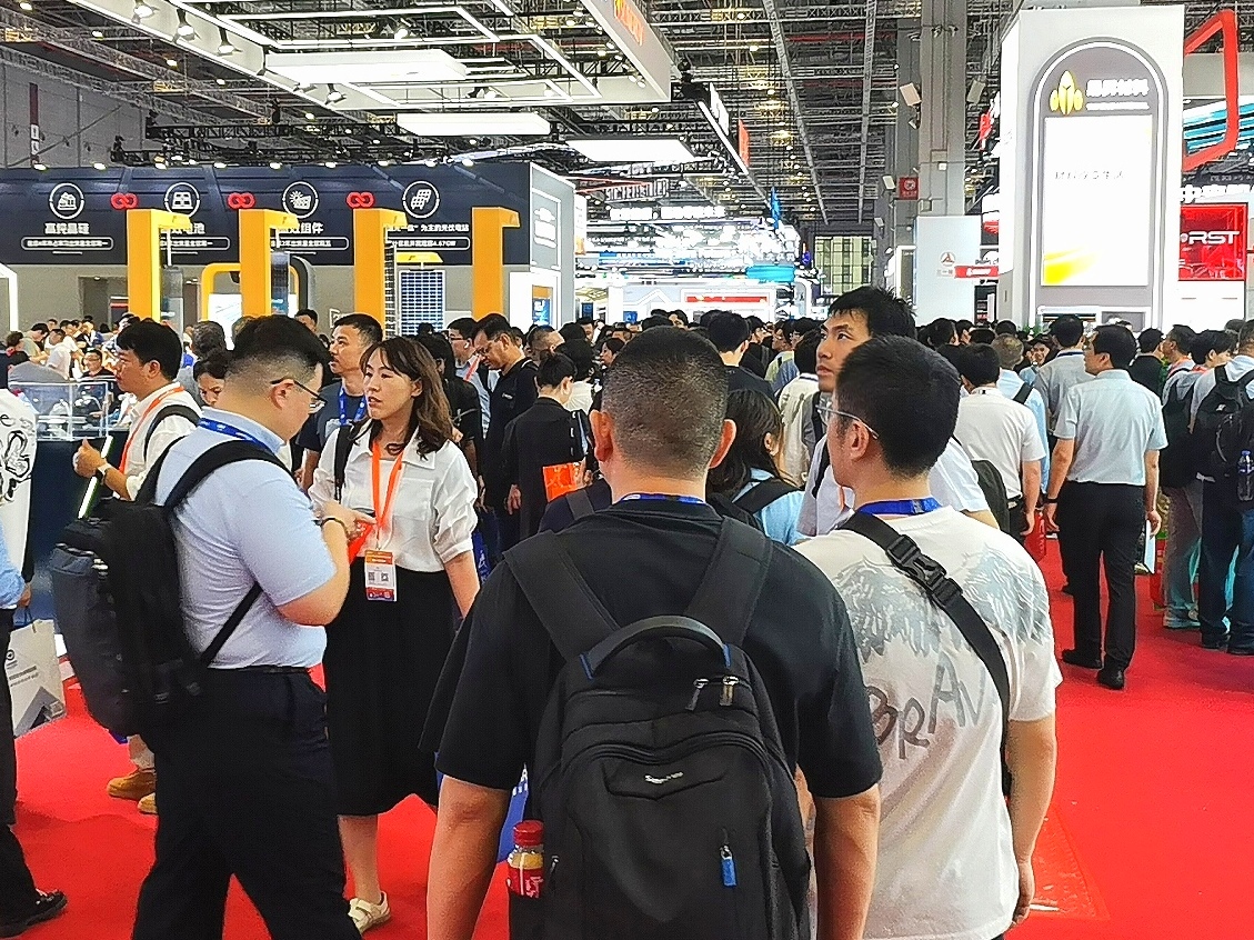
Related semiconductor industry manufacturers: From December 15th to 17th, 2026, the Shanghai International Semiconductor Industry Chain Exhibition will be held at the Shanghai New International Expo Center. As one of the largest semiconductor exhibitions in China, this exhibition is expected to attract more than 800 companies from around the world. We look forward to your visit.
The 2026 Shanghai International Semiconductor Industry Chain Exhibition will showcase the latest products and technologies in the semiconductor industry and applications, establish brand image for enterprises, promote trade cooperation and market development, lead industry trends, strengthen production, research and development, and sales interaction, deeply understand the new development trends of the semiconductor market in the future, explore new demands of the semiconductor market with a development perspective, innovate the exhibition content, and organize professional visitors from all aspects and levels, providing the best platform for technical exchange, product display, and trade negotiation for participating enterprises and merchants.
At the same time as the exhibition, an international semiconductor industry forum will be held, inviting domestic and foreign experts and representatives to interact and exchange ideas, discuss industry development trends, and share their experiences and achievements. At that time, we warmly welcome semiconductor manufacturers and related industry professionals from home and abroad to visit and exchange ideas.
Reason for participation:
Scale advantage, meeting new distributors and buyers: providing strong guarantee for exhibitors' actual exhibition effect. This exhibition is expected to attract over 40000 visitors and adopt a strong global investment promotion model. It will integrate databases from previous exhibitions and focus on inviting semiconductor industry users to visit and negotiate.
Seamless integration, inviting domestic and foreign merchants: There are advertising signs in the exhibition hall, subway stations, and hotels, which will directly introduce professional buyers involved in the field of this exhibition to our exhibition site for procurement negotiations.
※ Expand the market and consolidate existing market share: Enjoy comprehensive online and offline promotion throughout the year for one exhibition, covering new media such as websites, magazines, newspapers, mobile newspapers, Weibo, WeChat, etc. Multiple surprises for one exhibition. Keeping up with the latest market development trends, sharing and interacting, we have specially organized one-on-one trade matching meetings. We cordially invite purchasing managers from the semiconductor industry, both online and offline, with audiences from over 30 countries and regions around the world to arrange one-on-one meetings and negotiations, which is an excellent way to improve your product sales.
A hundred media outlets have been tracking and reporting on the entire process:
This exhibition places great emphasis on shaping and promoting the brand of exhibitors. By inviting central media, mainstream financial media, large portal websites, industry media, and overseas media to provide comprehensive, multi-dimensional, and three-dimensional coverage of exhibitors, it maximizes the promotion of the latest products and technologies to global buyers and creates unlimited business opportunities for exhibitors! This exhibition will invite hundreds of industry media outlets to report on site, including CCTV, Xinhua News Agency, China Business News, China Securities News, Securities Times, Phoenix Net, Sohu, NetEase, Sina, Tencent, etc.
Exhibition scope:
1. Semiconductor equipment: packaging equipment, diffusion equipment, welding equipment, cleaning equipment, testing equipment, refrigeration equipment, oxidation equipment, thinning machine, cutting machine, surface mount machine, single crystal furnace, oxidation furnace, grinding machine, heat treatment equipment, lithography machine, etching machine, polishing machine, chamfering machine, ion implantation equipment CVD/PVD equipment, coating/developing machines, front-end testing equipment, wet process equipment, thermal processing, coating equipment, single crystal deposition systems, solidification machines, plasma cleaning equipment, cutting machines, mounting machines, bonding machines, wire bonding machines, plastic packaging machines, reflow soldering, wave soldering, testing machines, bending equipment, sorting machines, robot automation, machine vision, other materials and electronic specialized equipment, coupling machines, carrier forming machines, testing equipment, constant temperature and humidity test chambers, sensors, packaging molds, testing fixtures, precision slide tables, stepper motors, valves, probe stations, clean room equipment, water treatment, etc;
2. IC design: IC and related electronic product design, IC product and application technology, IC testing methods and testing instruments, IC design and design tools, IC manufacturing and packaging, EDA, IP design, embedded software, digital circuit design, analog and mixed signal circuit design, integrated circuit layout design, IDM, Fabless factory, etc;
3. Wafer Manufacturing and Packaging: Wafer Manufacturing, SiP Advanced Packaging OSATs、EMS、OEMs、IDM、 Silicon wafers and IC packaging carriers, printed circuit boards, packaging substrates and equipment, assembly and testing, packaging design, testing, equipment and application manufacturing and packaging testing, etc EDA、MCU、 Printed circuit boards, packaging substrates, semiconductor materials and equipment, etc;
4. Integrated circuit manufacturing: wafer fabs, wafer foundries, analog integrated circuits, digital integrated circuits, hybrid integrated circuit manufacturing, integrated circuit terminal products, etc;
5. Packaging and testing accessories: testing probe station, probe card, testing machine, sorting machine, packaging equipment, packaging substrate, lead frame bonding wire, lead bonding, soldering testing, automation testing, laser cutting and others, grinding fluid, cutting fluid, sealing film (adhesive) high-temperature tape, laminated substrate, patch adhesive, feeding board, solder wire flow control, quartz graphite, silicon carbide, etc;
6. Third generation semiconductors: Third generation semiconductors such as silicon carbide (SiC), gallium nitride (GaN), wafers, substrates, packaging, testing, optoelectronic devices (LED), laser (LD), detector ultraviolet), power electronic devices (diode, MOSFET, JFET, BJT, IGBT, GTO, ETO, SBD, HEMT, etc.), microwave and radio frequency devices (HEMT, MMIC), etc;
7. Semiconductor materials: silicon wafers and silicon-based materials, silicon wafers, silicon wafers, monocrystalline silicon, silicon wafers, germanium silicon materials, S01 materials, silicon materials and compound semiconductor materials for solar cells, quartz products, graphite products, anti-static materials, photoresist and its supporting reagents, wafer tapes, photomasks, electronic gases, specialty chemical gases, CMP polishing materials, packaging substrates, lead frames, bonding wires, encapsulation materials, ceramic substrates, chip bonding materials, photoresist materials, wet electronic chemicals, sputtering targets, sealing materials, slicing, grinding, polishing, thin films, etc;
8. Electronic components: resistors, capacitors, potentiometers, electronic tubes, heat sinks, electromechanical components, connectors, semiconductor discrete devices/IGBTs, electroacoustic devices, laser devices, electronic display devices, optoelectronic devices, sensors, power supplies, switches, micro motors, electronic transformers, relays, printed circuit boards, integrated circuits, various circuits, piezoelectricity, crystals, quartz, ceramic magnetic materials, printed circuit substrates, electronic functional process specific materials, electronic adhesive (tape) products, electronic chemical materials and components, passive devices, 5G core components, special electronics, components, power management, storage, connectors, cables, plug-in devices, crystal oscillators, resistors, potentiometer magnetic components, filtering components PCB board, motor fan, electroacoustic device, display device, diode, transistor filter element, switch and component materials and equipment, etc;
New Technology Launch Conference, New Product Promotion Conference, Special Seminar:
If enterprises need to arrange such activities, please contact the organizing committee of the conference in a timely manner to arrange a better time slot.
Each session costs 30000 RMB and lasts for 1 hour (including various supporting facilities and promotional expenses).
Exhibition Tips:
1. Please fill out the "Exhibition Application and Contract" form carefully and stamp it with the official seal before returning it to the organizing committee.
2. After applying for a booth, exhibitors are required to wire transfer the booth fee to the designated account of the conference within 3 working days. After the remittance, the remittance receipt should be returned to the organizing committee for verification; If payment is not made in a timely manner within the specified time, the organizing committee will not reserve the original booth.
3. The principle of booth sequence allocation is "apply first, pay first, arrange first".
4. In order to ensure the overall image of the conference, the organizing committee reserves the final right to adjust the booths of some exhibitors.
Contact information of the organizing committee:
Postal Code: 201908
Phone: 157 2131 7652 (same WeChat number)
Contact: Xu Yang
Scope


Costs & Precautions
Contact
- Telephone:157 2131 7652
- Contact:Xu Yang
- Mobile:157 2131 7652
- Address:No. 2345 Longyang Road, Pudong New Area, Shanghai
Disclaimer
The information on this site comes from the network and related members, and the website has done its duty to review it. Due to the uncontrollability of the process of organizing the exhibition, some of the exhibition information in the station may change the subject matter, Extending or cancelling the event, please exhibitors and visitors must check with each other again before exhibiting! All the exhibitions in this site are not hosted/co-organized or organized, if there are any disputes during the exhibition, please hold the main responsibility of the exhibition organization! QQ Email: 523138820@qq.com WeChat: 523138820 Mobile: 15313206870


