


2025 Shenzhen Electronic Semiconductor · Greater Bay Area Semiconductor Exhibition
- Industry: Communications / Electronics
- Cycle: Annual
- Time: 2025/11/14 - 11/16 (Fri To Sun Total 3 Days) Error Correction
- Address: Shenzhen · Guangdong Shenzhen International Convention and Exhibition Center (New Building) ChinaGuangdong ProvinceShenzhenBaoan District No.1 Zhancheng Road, Fuhai Street, Bao'an District, Shenzhen
- Sponsor:2025 Shenzhen Electronic Semiconductor · Greater Bay Area Semiconductor Exhibition
- Organizer:2025 Shenzhen Electronic Semiconductor · Greater Bay Area Semiconductor Exhibition
Closed


- Contact:Zhang Dongxu
- E-mail:747852956@qq.com
- QQ:747852956
- Address:Room 314, Zone Z, 3rd Floor, Building 15, No. 7888 Waiqingsong Road, Qingpu District, Shanghai

INTRODUCTION


In the past few decades, the development of first and second generation semiconductors has enabled large enterprises in Europe, America, Japan, and South Korea. The efforts of the Chinese government and industry are expected to enhance China's position and voice in the latest generation semiconductor field. The huge demand and limited supply capacity have created great space for the development of the semiconductor industry in China. Despite the unpredictable external environment, the semiconductor industry still has long-term development potential, and this trend will continue to persist in the coming years.
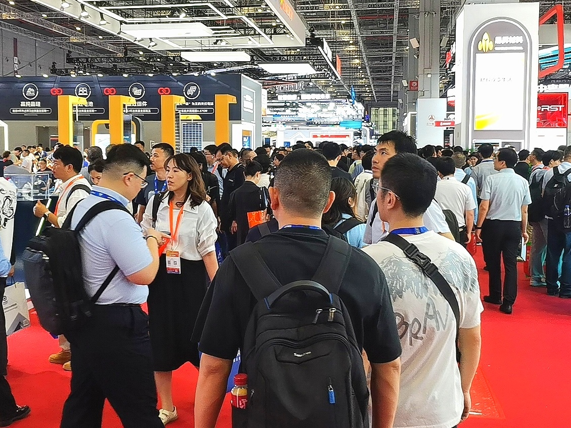
In order to better promote the development of the semiconductor industry and with strong support from national regulatory authorities, the 2025 China (Shenzhen) International Semiconductor Exhibition will be held from November 14-16, 2025 at the Shenzhen International Convention and Exhibition Center (Bao'an New Hall). This conference will adhere to the exhibition purpose of "highlighting brands, exploring innovation, and focusing on practical results". With unique creativity, scientific and reasonable integration and communication, and excellent services, it will provide a "high-level, high-grade, and high-quality" exhibition and communication stage for exhibitors with a new concept, and create the largest, most valuable, and authoritative top-level event in the semiconductor industry. We look forward to your participation in this exhibition.
Advantages of the Greater Bay Area
As China's manufacturing industry has shifted from high-speed growth to high-quality development, since 2013, the Chinese government has successively announced and promoted the "the Belt and Road" initiative and the construction of the "the Belt and Road" Greater Bay Area. The goal is to establish a new economic and trade partnership with countries along the "Belt and Road". At home, through the "Guangdong, Hong Kong and Macao Greater Bay Area", the Chinese government has accelerated the construction of a modern industrial system and multilateral open markets to drive high-quality development through continuous innovation. The construction of the "Guangdong Hong Kong Macao Greater Bay Area" refers to the development of nine cities in Guangdong Province (including Guangzhou, Shenzhen, Zhuhai, Foshan, Huizhou, Dongguan, Zhongshan, Jiangmen and Zhaoqing) and two special administrative regions of Hong Kong and Macao into world-class urban agglomerations and international scientific and technological innovation centers with global influence. By deepening the cooperation between Guangdong, Hong Kong and Macao and giving full play to their respective advantages, the Greater Bay Area will promote the coordinated development of regional economies and become an important support for the "the Belt and Road" to build a new platform for international economic cooperation. The GPD of the Greater Bay Area will reach 11.6 trillion yuan in 2019, and is expected to reach 28.9 trillion yuan by 2030, and squeeze into the world Among the top ten economies. The Guangdong Hong Kong Macao Greater Bay Area gathers high-quality resources from two regions, one province, and nine cities, and will be built into an international science and technology innovation center with global influence, a world-class advanced manufacturing industry, and a strategic emerging industry cluster area. It will become the fourth world-class bay area after New York, San Francisco, and Tokyo in the United States and Japan. The city cluster with the strongest innovation capability and the most open development potential is a gathering place for traditional manufacturing industries such as automobile manufacturing, new energy vehicles, semiconductors, and household appliances Consumer electronics, electronic information and equipment manufacturing, 5G materials, intelligent manufacturing, high-performance materials, energy conservation and environmental protection, etc.
Scope
1. Semiconductor equipment and intelligent equipment: packaging equipment, diffusion equipment, welding equipment, cleaning equipment, testing equipment, refrigeration equipment, oxidation equipment, thinning machine Slicer, SMT machine, monocrystalline furnace, oxidation furnace, grinding machine, heat treatment equipment, lithography machine, etching machine, polishing machine, chamfering machine, ion implantation equipment CVD/PVD equipment, coating/developing machines, front-end testing equipment, wet process equipment, thermal processing, coating equipment, single crystal deposition systems, solidification machines, plasma cleaning equipment, cutting machines, mounting machines, bonding machines, wire bonding machines, plastic packaging machines, reflow soldering, wave soldering, testing machines, bending equipment, sorting machines, robot automation, machine vision, other materials and electronic specialized equipment, coupling machines, carrier forming machines, testing equipment, constant temperature and humidity test chambers, sensors, packaging molds, testing fixtures, precision slide tables, stepper motors, valves, probe stations, clean room equipment, water treatment, etc. 2. Wafer manufacturing and packaging: wafer manufacturing, SiP advanced packaging, The sentence is: OSATS、EMS、OEMS、IDM、 Silicon wafers and IC packaging carriers, printed circuit boards, packaging substrates and equipment, assembly and testing, packaging design, testing, equipment and application manufacturing and packaging testing, etc EDA、MCU、 Printed circuit boards, etc; 3. Packaging and testing accessories: testing probe station, probe card, testing machine, sorting machine, packaging equipment, packaging substrate, lead frame bonding wire, lead bonding, soldering testing, automation testing, laser cutting and others, grinding fluid, cutting fluid, sealing film (adhesive) high-temperature tape, laminated substrate, patch adhesive, feeding board, solder wire flow control, quartz graphite, silicon carbide, etc;
4. IC design: IC and related electronic product design, IC product and application technology, IC testing methods and testing instruments, IC design and design tools, IC manufacturing and packaging, EDA, P design, embedded software, digital circuit design, analog and mixed signal circuit design, integrated circuit layout design, IDM, Fabless factory, etc.: 5. Integrated circuits: wafer manufacturing plants, wafer foundries, analog integrated circuits, digital integrated circuits and mixed signal integrated circuit manufacturing, integrated circuit terminal products, etc.:
6. Semiconductor materials: silicon wafers and silicon-based materials, silicon wafers, silicon wafers, monocrystalline silicon, silicon wafers, germanium silicon materials, S01 materials, silicon materials and compound semiconductor materials for solar cells, quartz products, graphite products, anti-static materials, photoresist and its supporting reagents, wafer tapes, photomasks, electronic gases, specialty chemical gases, CMP polishing materials, packaging substrates, lead frames, bonding wires, encapsulation materials, ceramic substrates, chip bonding materials, photoresist materials, wet electronic chemicals, sputtering targets, sealing materials, slicing, grinding, polishing, thin films, etc; 7. Third generation semiconductors: Third generation semiconductors such as silicon carbide (Si ℃), gallium nitride (GaN), wafers, substrates, packaging, testing, optoelectronic devices (light-emitting diodes (LEDs), lasers (LD), detectors (UV)), power electronic devices (diodes, MOSFETs, JFETs, BJTs, IGBTs, GTOs, ETOs, SBDs, HEMTs, etc.), microwave and radio frequency devices (HEMTs, MMICs), etc.:
8. Electronic components: resistors, capacitors, potentiometers, electronic tubes, heat sinks, electromechanical components, connectors, semiconductor discrete devices/GBTs, electroacoustic devices, laser devices, electronic display devices, optoelectronic devices, sensors, power supplies, switches, micro motors, electronic transformers, relays, printed circuit boards, integrated circuits, various circuits, piezoelectric, crystal, quartz, ceramic magnetic materials, printed circuit substrate substrates, electronic functional process specific materials, electronic adhesive (tape) products Electronic chemical materials and components, passive components, 5G core components, special electronics, components, power management, storage devices, connectors, cables, plug-in devices, crystal oscillators, resistors, potentiometer magnetic components, filtering components, PCB boards, motor fans, electroacoustic devices, display devices, diodes, transistor filtering components, etc;
Costs & Precautions
Please contact the exhibition organizer before participating in the exhibition to confirm.


Contact
- Contact:Zhang Dongxu
- E-mail:747852956@qq.com
- QQ:747852956
- Address:Room 314, Zone Z, 3rd Floor, Building 15, No. 7888 Waiqingsong Road, Qingpu District, Shanghai
Disclaimer
The information on this site comes from the network and related members, and the website has done its duty to review it. Due to the uncontrollability of the process of organizing the exhibition, some of the exhibition information in the station may change the subject matter, Extending or cancelling the event, please exhibitors and visitors must check with each other again before exhibiting! All the exhibitions in this site are not hosted/co-organized or organized, if there are any disputes during the exhibition, please hold the main responsibility of the exhibition organization! QQ Email: 523138820@qq.com WeChat: 523138820 Mobile: 15313206870


加载中...
加载中...
